Dual Beam FIB
Home » Our Techniques » Imaging » Dual Beam – FIB
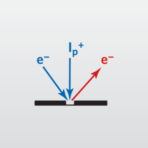
A Focused Ion Beam (FIB) instrument uses a finely focused ion beam to modify and image the sample of interest. FIB is chiefly used to create very precise cross sections of a sample for subsequent imaging via SEM, STEM or TEM or to perform circuit modification. Additionally, FIB imaging can be used to image a sample directly, detecting emitted electrons either from the ion or electron beam. The contrast mechanism for FIB is different than for SEM or S/TEM, so unique structural information can be obtained in some cases. A dual beam FIB/SEM integrates these two techniques into one tool whereas a single beam FIB contains only an ion beam, with electron beam imaging taking place in a separate SEM, STEM or TEM instrument.
As a sample preparation tool, the FIB can accurately produce cross-sections of a sample that are impossible to create otherwise:
- FIB analysis has revolutionized sample preparation for TEM samples, making it possible to identify sub-micron features and precisely prepare cross sections.
- FIB-prepared sections are used extensively in SEM microscopy, where the FIB preparation, SEM imaging, and elemental analysis can happen with the same multi-technique tool.
- FIB-prepared sections are also used in Auger Electron Spectroscopy to provide elemental identification of subsurface features quickly and precisely.
- It is an ideal tool for examining products with small, difficult-to-access features, such as those found in the semiconductor industry and for sub-surface particle identification.
- It is a good option for products that are hard to cross section, such as a soft polymer that is challenging to polish.
Ideal Uses of FIB
- SEM, STEM and TEM sample preparation
- High resolution cross-section images of small, hard-to-access sample features
- Micro sampling via in-situ liftout
Strengths
- Best method to cross-section small targets
- Rapid, high-resolution imaging
- Good grain contrast imaging
- Versatile platform that supports many other tools
Limitations
- Vacuum compatibility typically required
- Imaging may spoil subsequent analyses
- Residual Ga on analytical face
- Ion beam damage may limit image resolution
- Cross-section area is small
FIB Technical Specifications
- Signals Detected: Electrons, secondary ions, X-rays, light (Cathodoluminescence)
- Imaging/Mapping: Yes
- Lateral Resolution/Probe Size: 7 nm (ion beam); 20 nm (electron beam)
Related Resources
Would you like to learn more about using Dual Beam FIB?
Contact us today for your Dual Beam FIB needs. Please complete the form below to have an EAG expert contact you.