Transmission Electron Microscopy (TEM) and Scanning Transmission Electron Microscopy (STEM)
Home » Our Techniques » Imaging » TEM-STEM
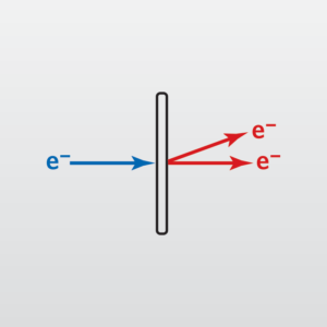
Transmission Electron Microscopy (TEM analysis) and Scanning Transmission Electron Microscopy (STEM) are similar techniques that image a sample using an electron beam. Image resolutions are around 1-2 Å for TEM and STEM analysis. High-energy electrons (80-200 keV) are transmitted through electron transparent samples (~100 nm thick). TEM and STEM have better spatial resolution than SEM but often require more complex sample preparation.
Though TEM and STEM are more time intensive than many other frequently used analytical tools, a variety of signals are accessible from these techniques, making it possible to perform chemical analysis at the nano scale. Besides high image resolutions, it is possible to characterize crystallographic phase, crystallographic orientation (using electron diffraction experiments), generate elemental maps (by using EDS or EELS) and acquire images highlighting elemental contrast (Z-contrast or HAADF-STEM mode). These can all be accomplished from precisely located areas at the nm scale. STEM and TEM are excellent failure analysis tools for thin film and IC samples.
Ideal Uses
- Metrology at 0.2 nm resolution
- Identification of nm-sized defects on integrated circuits, including embedded particles and via residues
- Determination of crystallographic phases at the nanometer scale
- Nanoparticle characterization: size, core/shell investigations, agglomeration, effects of annealing…
- Catalyst studies
- Nanometer scale elemental maps
- III-V super lattice characterization
- Crystal defect characterization (dislocations, grain boundaries, voids, stacking faults)
Strengths
- The highest spatial resolution elemental mapping of any analytical technique
- Sub 0.2 nm (2 Å) image resolution
- Small area crystallographic information
- Strong contrast between crystalline vs. amorphous materials without chemical staining
Limitations
- Significant sample preparation time (1-4 hrs)
- Small sampling volumes. Samples are typically ~100 nm thick and 5×5 μm
- Some materials are not stable in the high energy electron beam
TEM & STEM Technical Specifications
- Signals Detected: Transmitted electrons, scattered electrons, secondary electrons, x-rays
- Elements Detected: B-U (EDS)
- Detection Limits: 0.1-1 at%
- Imaging/Mapping: Yes (EDS, EELS)
- Ultimate Lateral Resolution: <0.2 nm
Would you like to learn more about using TEM and STEM?
Contact us today for your Transmission Electron Microscopy and Scanning TEM needs. Please complete the form below to have an EAG expert contact you.